Semiconductors, Electronics & IoT
Supporting the sensing of the IoT Age with the manufacture of semi conductors and electronic parts
Thin-film technology has proven useful to the continued evolution of semi conductor and electronic parts manufacturing, along with its IoT applications
In the IoT age, people and things are connected through networks, everywhere we go. As Big data that proves useful to lifestyle, social activities, and business intersects, the necessity for massive information processing, such as AI analysis, means that semi conductors and electronic parts play an increasingly important role.
Geomatec's unique high-performance thin-film technology has relieved the yield of semi conductor and electronic part manufacturing, while also contributing to greater quality and the evolution of our information society, all while providing sensors fit for the IoT age.
Manufacture of Semi Conductors & Electronic Parts
Fan out panel level packaging (FOPLP)
Enabling the spread of semi-conductor manufacturing through next-level packaging technology
MITSUI MINING & SMELTING CO., LTD.'s fine circuit forming material with glass carrier, HRDP®, was developed to contribute to the spread of fan out panel level packages (FOPLP), a next-generation packing technology.
This material involves applying multiple layers of thin film to the surface of a glass carrier, while Geomatec provided the ultrafine RDL necessary to form super-thin seed layers for plating and a lift-off function layer that is stable even at thermal loads of 260℃, which enables the mechanical removal of the glass carrier. By exceeding the boundaries of traditional processing, this has contributed to the high integration and micro fabrication of next-generation semi-conductors, increasing yield and production efficiency.
Related Products & Solutions
IoT Sensors
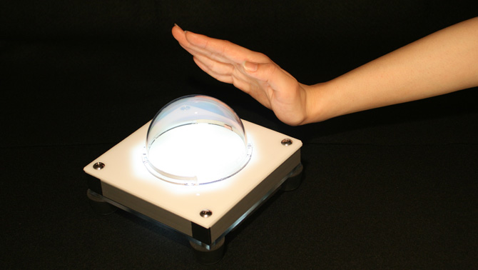
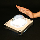
Capacitive proximity sensors
Transparent and non-contact, enabling detection of a range of movements
When Geomatec's high-performance thin-film technology is applied to capacitive proximity sensors, it is possible to detect the changes in capacitance that occur between the sensor's transparent electrodes, water, and matter such as human bodies. These functions can be applied in both sensors and switches to create products such as sensors that monitor water levels or electrical power switches that can be turned on and off simply with the movement of a hand.
For example, a light that switches on or grows in intensity when people approach a transparent dome, or one that dims when people move away from it, enabling sensitive control.
Related Products & Solutions
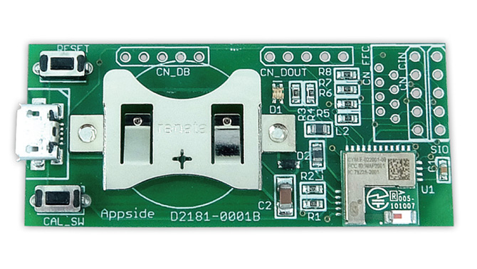
IoT development kit for BLE capacitive proximity sensors
Easily detect changes in capacitance from a distance with Bluetooth® compatibility
Geomatec's capacitive proximity sensor technology was used in the IoT development Kit for BLE capacitive proximity sensors (Cooperation and sale: Bit Trade One, LTD)
IoT evaluation boards are created in miniature sizes, capable of fitting into a child's hands, and are also capable of short-range wireless communication via Bluetooth® Low Energy. The sensitivity threshold can be adjusted with a smart phone (iOS) application, while the sensors themselves are available in a wide variety of types, such as close-proximity sensors and touch sensors that respond when an object passes near them, enabling easy experimentation and validation.
Related Products & Solutions
There are even more uses for thin-film technology, beyond the above
Unpublished and undisclosed information exists beyond the above. Uses for Geomatec's thin-film technology continue to expand.
In order to realize your ideas, please feel free to contact us for advice.