Geomatec to provide thin film for "HRDP®", the material for formation of ultra-fine circuits developed by MITSUI MINING & SMELTING CO.,LTD. for use with fan out wafer level packaging
NewsJanuary 25, 2018
Geomatec announced that it has established a technique for employing thin films in the mass production of HRDP®*, the material for formation of ultra-fine circuits developed by MITSUI MINING & SMELTING CO.,LTD. (President and CEO Keiji Nishida) for use with fan out panel level packages.
MITSUI MINING & SMELTING CO.,LTD. (below, Mitsui Mining) developed HRDP® for fan out panel level packaging, a revolutionary technique that meets the high performance demands of the IoT age. Geomatec will provide Mitsui Mining with a mass production technique for HRDP® that uses multiple layers of high performance thin film. As professionals in the field of high-value thin film and processing technology, Geomatec has engaged in cooperation and co-production with Mitsui Mining to ensure adequate supply capacity.
*High Resolution De-bondable Panel
About HRDP®
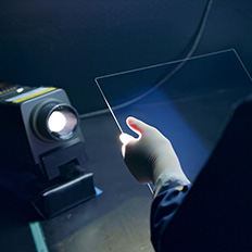
HRDP® is created by applying multiple layers of thin film to the surface of a glass carrier (Photo 1, Figure 1).
The "seed layers for plating" applied to the highly flat surface of the glass carrier enable the highly sensitive RDL* to be fabricated at panel size (Ex: 600x600 mm). In addition, the "release layer" ensures that safe mechanized removal of the glass carrier can be carried out, even after reaching a thermal load of 260℃.
*Re-Distribution Layer
-
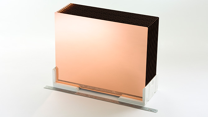
Photo 1: External surface of "HRDP®" -
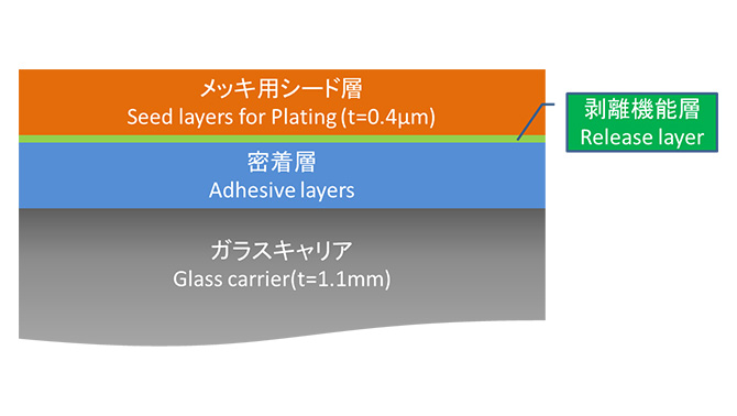
Figure 1: Schematic diagram of "HRDP®" cross-sectional structure
Inquiries
Please feel free to contact us for any further questions.
Contact Us